

-
Products -PCBA Manufacturing RF Connectors RF Cable Assemblys Embedded Antennas External Antennas GNSS Positioning Solutions
RF Connectors

RF Cable Assemblys
Embedded Antennas
External Antennas
GNSS Positioning Solutions




 Language


Language


Time:2026-10-15 Views:0
Why Precision Defines Performance
In the rapidly evolving world of wireless communication, satellite navigation, and autonomous systems, the performance of a receiver board is only as good as the precision with which it is assembled. High precision receiver board assembly has emerged as a critical discipline that bridges advanced circuit design and realworld operational reliability. From centimeterlevel GNSS positioning to missioncritical RF signal reception in aerospace applications, the manufacturing tolerances, material selections, and assembly processes directly determine whether a receiver performs to specification—or fails in the field.
The global GNSS OEM board market alone is projected to grow from US$4.5 billion in 2025 to US$7.7 billion by 2032, reflecting the surging demand for highaccuracy positioning solutions across industries including autonomous vehicles, precision agriculture, surveying, and telecommunications infrastructure. This growth underscores a fundamental reality: as receiver technology becomes more sophisticated, the manufacturing precision required to produce these boards becomes equally demanding.
This comprehensive guide explores every dimension of high precision receiver board assembly—from the fundamental precision requirements and material science considerations to advanced manufacturing processes, rigorous testing protocols, and the strategic supply chain decisions that separate industry leaders from laggards.
Understanding High Precision Receiver Board Assembly
What Constitutes "High Precision"?
High precision receiver board assembly is not merely a marketing term—it represents a quantifiable set of manufacturing standards that directly impact electrical performance. In the context of RF and GNSS receiver boards, precision manifests across multiple dimensions:
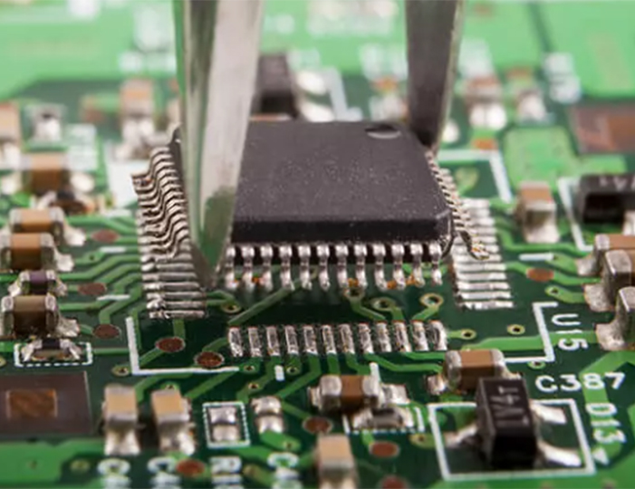
Component placement accuracy is measured in microns. Modern highprecision pickandplace machines achieve placement accuracy of ±0.025 mm, but even this level of precision must be complemented by rigorous verification. Industry data indicates that placement deviation exceeding 0.05 mm can cause measurable degradation in signal reception sensitivity, particularly for finepitch RF components and multiband antenna interfaces.
Assembly tolerances in specialized applications push the boundaries even further. Research on spaceborne extremely highfrequency receiver components has demonstrated assembly accuracy of 50 μm, achieved through careful management of thermal expansion mismatches between RF inserts and aluminum housings. This level of precision is not academic—it directly enables satellite communication systems to function reliably in the extreme thermal cycling environment of space.
Impedance control represents another critical precision parameter. Every solder joint, every trace routing decision, and every shield placement affects the characteristic impedance of RF signal paths. Variations as small as a few percent can introduce signal reflections, insertion loss, and phase distortion that degrade receiver sensitivity and positioning accuracy.
The Distinction Between Standard and High Precision Assembly
Not all receiver boards require the same level of precision. Standard commercial receiver assemblies may tolerate placement deviations of 0.1 mm and impedance variations of ±10%, sufficient for consumer audio receivers or basic telemetry applications. High precision receiver board assembly, by contrast, operates under far tighter constraints:
Finepitch components with 0.4 mm or smaller lead spacing demand placement accuracy better than ±0.03 mm
RFsensitive layouts require controlled impedance within ±5% across the entire signal chain
Multilayer stackups with 8 to 14 layers demand registration tolerances under 50 μm
Shielding and grounding must achieve isolation exceeding 60 dB in critical frequency bands
Thermal management requires voidfree die attach and controlled thermal expansion matching
The distinction is not trivial. A standard assembly process might yield a receiver board that functions adequately in laboratory conditions. A high precision assembly process produces a receiver board that maintains specificationlevel performance across temperature extremes, vibration, humidity, and years of continuous operation.
Precision Requirements in Receiver Board Design
RF Signal Integrity: The Foundation of Precision
RF signal integrity is the single most demanding precision requirement in receiver board assembly. Unlike digital circuits, which tolerate considerable noise margins, RF receivers operate at signal levels often measured in microvolts. Any degradation in the signal path—whether from parasitic capacitance, poor grounding, or impedance discontinuities—directly translates to reduced sensitivity, increased noise figure, and degraded positioning accuracy.
The manufacturing implications are profound. Every component placement must maintain the designed electrical length of RF traces. Every solder joint must exhibit consistent geometry to avoid impedance variations. Every ground via must provide a lowinductance path to the reference plane. These requirements are not achievable through standard SMT processes alone—they demand a manufacturing partner with deep RF expertise and specialized process controls.
Component Placement Accuracy and Its Consequences
Component placement accuracy in high precision receiver board assembly extends far beyond simply "getting the part on the pad." For RFcritical components such as lownoise amplifiers, mixers, and filters, placement deviation affects:
1. Impedance matching networks: A 0.05 mm shift in a matching capacitor position can shift the resonant frequency of a matching network by several MHz, degrading return loss and increasing insertion loss.
2. Phase relationships: In multichannel receivers used for angleofarrival calculations or beamforming, phase matching between channels is critical. Placement variations introduce phase errors that degrade angular accuracy.
3. Thermal pathways: For highpower RF components, precise placement ensures proper thermal contact with heatspreading structures, preventing localized hot spots that accelerate component degradation.
Impedance Control and Signal Loss Minimization
Controlled impedance is not a PCB fabrication concern alone—it is a holistic design and assembly challenge. The characteristic impedance of an RF trace is determined by trace width, dielectric thickness, dielectric constant, and the presence of nearby conductors. During assembly, each of these parameters can be affected:
Solder mask thickness over RF traces varies with application method and can shift impedance by several percent
Component placement affects the effective electrical length of traces between components
Shield can attachment introduces parasitic capacitance that must be accounted for in the design
Via placement and filling in ground structures affects the inductance of return paths
High precision assembly processes address these variables through rigorous process control, including solder mask thickness verification, impedance testing of test coupons, and Xray inspection of via quality.
Materials and Components for High Precision Assembly
PCB Materials: The Substrate Matters
The choice of PCB substrate material is fundamental to receiver board performance. Standard FR4, while economical and widely available, exhibits dielectric losses that become problematic at frequencies above 3 GHz. For high precision receiver boards, alternative materials are essential:
PTFEbased laminates such as Rogers RT/duroid series offer low dielectric constant (εr ≈ 2.2–3.0) and extremely low loss tangent (tan δ < 0.001), making them ideal for multiband GNSS receivers operating across L1, L2, and L5 frequencies. However, these materials present assembly challenges: their high coefficient of thermal expansion (CTE) requires careful thermal management during soldering, and their soft surface demands specialized handling to prevent damage.
Hydrocarbon ceramic laminates provide a middle ground, offering dielectric constants in the range of 3.0–3.5 with loss tangents below 0.002. These materials exhibit better dimensional stability than PTFE and are compatible with standard PCB assembly processes, making them popular for highvolume precision receiver production.
Ceramic substrates such as alumina (Al₂O₃) and aluminum nitride (AlN) are used in the most demanding applications, particularly for spaceborne and military receiver assemblies. These materials offer exceptional thermal conductivity and dimensional stability but require specialized assembly techniques including eutectic die attach and thinfilm metallization.
Solder Materials and Thermal Management
The solder alloy selection for high precision receiver assembly involves tradeoffs between melting temperature, mechanical properties, and thermal conductivity. For RF power components and thermally sensitive assemblies, the choice of solder can determine whether the receiver meets its performance specifications.
Leadfree solders such as SAC305 (Sn96.5/Ag3.0/Cu0.5) are increasingly mandated by environmental regulations but require higher reflow temperatures (peak 245–250°C) that can stress thermally sensitive components. Their higher melting point also creates challenges for assemblies that undergo subsequent processing steps.
Eutectic tinlead solders (Sn63/Pb37) remain in use for aerospace and defense applications where their predictable melting behavior and proven reliability outweigh environmental considerations. Their lower melting point (183°C) reduces thermal stress on components during assembly.
Goldtin eutectic (Au80/Sn20) is used for die attach in highreliability applications, offering excellent thermal conductivity and voidfree bonding at temperatures around 300°C. This material is particularly relevant for spaceborne receiver assemblies where thermal cycling reliability is paramount.
Conductive epoxies provide an alternative for temperaturesensitive assemblies, offering roomtemperature or lowtemperature curing. While their electrical conductivity is lower than metallic solders, advances in silverfilled epoxy formulations have made them viable for many RF applications, including substrate attachment and component bonding.
Component Selection for Precision
The passive and active components used in high precision receiver boards must meet stringent specifications:
Resistors require 1% tolerance or better for critical matching networks; temperature coefficient of resistance (TCR) should be below 50 ppm/°C
Capacitors must exhibit low ESR and ESL, with NP0/C0G dielectrics preferred for frequencydetermining elements
Inductors require high Q and tight tolerance, with aircore or ceramiccore construction for minimal loss
Oscillators demand exceptional frequency stability, typically better than ±0.5 ppm over temperature and aging
LNAs and mixers must be selected for noise figure and linearity, with careful attention to package parasitics
The High Precision Assembly Process
SMT Process Control for RF Assemblies
Surface mount technology (SMT) forms the backbone of modern receiver board assembly, but standard SMT processes are insufficient for high precision applications. The following process controls are essential:
Solder paste deposition must be precisely controlled in volume and placement. Stencil design requires careful attention to aperture size, wall geometry, and surface finish. Lasercut, electropolished stainless steel stencils with trapezoidal walls are recommended to ensure clean paste release and consistent deposit volume. For finepitch components, stencil thickness may be reduced to 0.10 mm or less to prevent bridging.
Pickandplace operations demand machines capable of simultaneous high speed and high accuracy. Modern placement systems achieve repeatability better than ±0.025 mm at speeds exceeding 20,000 components per hour. Vision systems with fiducial recognition and component centering ensure placement accuracy even for microBGA and QFN packages.
Reflow profiling must be optimized for each assembly, accounting for component thermal mass, PCB thickness, and solder alloy characteristics. For mixedtechnology assemblies containing both RF and digital components, the profile must balance the need for complete solder melting against the risk of thermal damage to sensitive devices.
3D SPI (Solder Paste Inspection) and AOI (Automated Optical Inspection) provide closedloop quality control, detecting paste deposition anomalies and placement errors before they become permanent defects.
Selective Soldering and Hand Assembly Considerations
Despite advances in SMT automation, certain receiver board components require selective soldering or hand assembly:
Connectors with high pin counts or mixed technology may require selective wave soldering
Shield cans are often attached after primary reflow to avoid thermal damage to internal components
Temperaturesensitive components may require hand soldering with controlled tip temperature
RF cable assemblies demand precision hand soldering or specialized connector attachment processes
Each of these operations must be performed by operators trained in RF assembly techniques, using temperaturecontrolled soldering stations with fine tips and appropriate flux chemistries. Visual inspection under magnification is essential, as is electrical verification at each assembly stage.
Shielding and Grounding Assembly
Shielding is critical for receiver boards operating in electromagnetically hostile environments. The assembly of shield cans and grounding structures requires particular attention:
Shield can attachment must provide continuous electrical contact around the perimeter, typically achieved through soldering or conductive gasket compression
Ground via arrays beneath shield cans must be dense enough to prevent resonant cavity effects
Component clearance inside shields must account for thermal expansion and vibration
Shield removal for rework must be possible without damaging the board or components
The effectiveness of shielding is often verified through nearfield scanning or radiated emissions testing, with isolation targets typically exceeding 60 dB in critical frequency bands.
Thermal Management in Precision Assemblies
Thermal management is both a design and assembly concern. Highpower RF components generate heat that must be conducted away from the junction to maintain performance and reliability. Assemblyrelated thermal considerations include:
Die attach voiding: Voids in the thermal interface between a die and its package or between a package and the PCB significantly increase thermal resistance. Xray inspection is essential for verifying voidfree attachment.
Thermal via quality: Vias used for thermal conduction must be properly filled and plated to achieve their designed thermal resistance.
Heat sink attachment: For highpower receivers, the interface between the PCB and heat sink must be uniform and voidfree, often requiring thermal interface materials (TIMs) with controlled thickness.
Testing and Verification Protocols
RF Performance Testing
Testing is not an afterthought in high precision receiver board assembly—it is an integral part of the manufacturing process. RF performance testing verifies that the assembled board meets its design specifications:
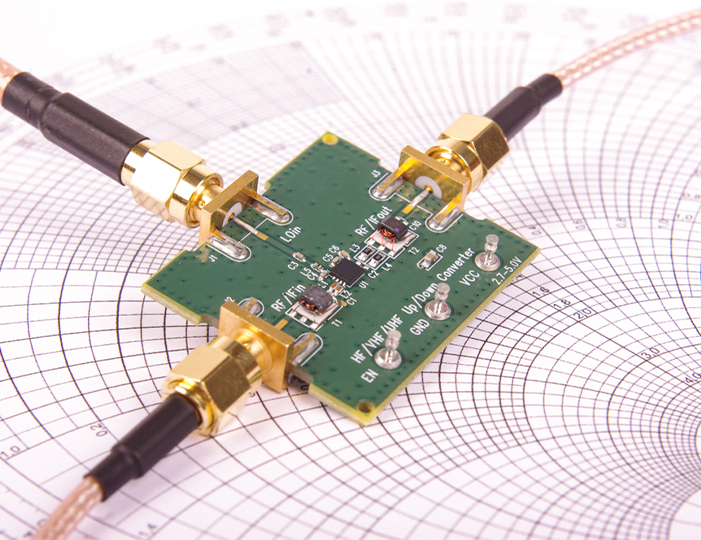
Sparameter measurements verify impedance matching and insertion loss across the operating frequency band
Noise figure measurement confirms receiver sensitivity
Gain and phase matching ensure multichannel receivers meet phase accuracy requirements
Isolation testing verifies channeltochannel and shieldtoshield isolation
Spurious response testing identifies unwanted emissions or responses
These tests require calibrated vector network analyzers, noise figure meters, and specialized RF test fixtures. The test setup itself introduces measurement uncertainties that must be characterized and accounted for.
Environmental Stress Screening
High precision receiver boards destined for demanding applications must undergo environmental stress screening (ESS) to identify latent defects:
Thermal cycling (55°C to +125°C) accelerates failure mechanisms related to CTE mismatches
Vibration testing simulates launch and operational vibration environments
Humidity exposure verifies resistance to moistureinduced degradation
Thermal vacuum testing is essential for spaceborne assemblies
ESS is particularly important for spaceborne and aerospace receiver assemblies, where field repair is impossible. The assembly process must produce boards that survive these stresses without degradation.
Functional Testing and Calibration
Functional testing verifies that the complete receiver board operates as intended, including:
Positioning accuracy verification for GNSS receivers, typically requiring RTK or PPP test setups
Timetofirstfix measurement
Signal acquisition sensitivity testing
Calibration of oscillators, filters, and gain stages
For GNSS receiver boards, functional testing often involves connection to a GNSS simulator or a reference antenna with known position, allowing precise verification of positioning accuracy and timing performance.
Challenges and Solutions in High Precision Receiver Assembly
Managing Thermal Mismatch in Heterogeneous Assemblies
One of the most persistent challenges in high precision receiver assembly is managing thermal expansion mismatches between dissimilar materials. RF connectors, ceramic substrates, and aluminum housings all expand at different rates when subjected to temperature changes. Research on spaceborne receiver assemblies has demonstrated that careful design of the thermal interface between RF inserts and aluminum housings can resolve these mismatches, achieving assembly accuracy of 50 μm even under thermal cycling.
Solutions include:
Compliant interface materials that accommodate differential expansion
Matched CTE materials where possible, such as aluminum nitride substrates matched to aluminum housings
Controlled assembly temperatures that minimize residual stresses at room temperature
Finite element analysis to predict thermal stresses before physical prototyping
Component Attachment Void Prevention
Void formation beneath components during soldering is a persistent challenge that directly affects electrical and thermal performance. A critical issue in conventional soldering processes is the formation of unwanted voids beneath components, which affects gain and phase performance of receiver systems.
Prevention strategies include:
Optimized reflow profiles that allow volatiles to escape before solder solidification
Vacuumassisted soldering for critical die attach applications
Solder preforms with controlled geometry for consistent joint formation
Flux selection that minimizes outgassing during reflow
Xray inspection at 100% for critical attachment interfaces
Supply Chain and Component Availability
The supply chain for highprecision receiver components has become increasingly complex. Critical RF components—particularly those from a limited number of qualified suppliers—face extended lead times and allocation challenges. Supply disruptions can force alternative component selection, which in turn may introduce new power or performance considerations that affect assembly processes.
Mitigation strategies include:
Early engagement with component suppliers and authorized distributors
Design for multiple sources where technically feasible
Buffer inventory of longlead critical components
Alternative component qualification programs to preapprove substitutes
Close collaboration between design and manufacturing teams to evaluate supply chain implications of design decisions
Applications Driving Precision Requirements
GNSS and Satellite Navigation
GNSS receivers represent the largest and most rapidly growing application for high precision assembly. Modern multifrequency, multiconstellation receivers must process signals from GPS, GLONASS, Galileo, BeiDou, QZSS, and NavIC across multiple frequency bands, including Lband corrections. The assembly precision requirements for these boards are driven by:
Centimeterlevel positioning accuracy demands phasestable signal paths across all frequency bands
Multipath rejection requires excellent antenna and frontend performance
Jamming and spoofing detection relies on precise phase and amplitude matching between multiple antenna channels
RTK and PPP processing requires consistent group delay across all received signals
Autonomous Systems and Robotics
Autonomous vehicles, drones, and industrial robots rely on high precision GNSS receivers for navigation and control. The assembly precision of these receiver boards directly affects:
Lanelevel navigation accuracy for autonomous driving
Hover stability and waypoint accuracy for UAVs
Path repeatability for agricultural robots and autonomous machinery
Safetycritical positioning for industrial automation
Telecommunications and Timing Synchronization
5G and future 6G networks require precise timing synchronization, often derived from GNSS receivers. The assembly precision of these timing receivers affects:
Network synchronization accuracy, typically better than 1 μs
Holdover stability during GNSS outages
Phase noise performance for highorder modulation schemes
Longterm reliability in uncontrolled environmental conditions
Aerospace and Defense
Spaceborne and airborne receiver assemblies represent the most demanding application for precision manufacturing. These assemblies must survive:
Launch vibration exceeding 10 Grms
Thermal vacuum environments with extreme temperature cycling
Radiation exposure that can degrade component performance
Extended mission durations of 15 years or more
The assembly precision achieved in these applications—50 μm positional accuracy and voidfree die attach—represents the state of the art in receiver board manufacturing.
Selecting a High Precision Assembly Partner
Capabilities to Evaluate
Selecting the right manufacturing partner is arguably the most important decision in developing a high precision receiver product. Key capabilities to evaluate include:
Technical expertise: Does the partner have demonstrated experience with RF and microwave assemblies? Can they discuss impedance control, shielding effectiveness, and thermal management with authority?
Process capability: What placement accuracy can they achieve? What inspection equipment do they have? Can they provide process capability data (Cpk) for critical operations?
Quality systems: Are they certified to relevant standards such as IPCA610 Class 3, IATF 16949, or AS9100? Do they have a documented quality management system that covers all aspects of production?
Testing capabilities: Can they perform inhouse RF testing, or do they rely on external test houses? What test equipment and calibration procedures do they use?
Supply chain management: How do they manage component sourcing, especially for longlead or singlesource components? Do they have established relationships with authorized distributors?
Scalability: Can they support prototype quantities as well as volume production? What is their capacity for rampup?
Questions to Ask Potential Partners
When evaluating assembly partners, these questions reveal capabilities and priorities:
1. What is your documented placement accuracy for finepitch components?
2. How do you verify impedance control on RF assemblies?
3. What is your process for shield can attachment and verification?
4. How do you manage thermal mismatch in heterogeneous assemblies?
5. What percentage of your production undergoes 100% electrical test?
6. How do you handle engineering changes and rework?
7. What is your typical lead time for prototype and production quantities?
8. Can you provide references from customers with similar RF assembly requirements?
Red Flags and Warning Signs
Certain warning signs suggest a partner may not be suited for high precision receiver assembly:
Inability to discuss RFspecific process controls in technical terms
Lack of inhouse RF testing capabilities
No documented process capability data for critical operations
Reliance on visual inspection alone for quality verification
High employee turnover in technical positions
Limited experience with the specific frequency bands or package types required
Future Trends in High Precision Receiver Assembly
Advanced Packaging Technologies
The relentless demand for smaller, more capable receiver boards is driving adoption of advanced packaging technologies:
SysteminPackage (SiP) integrates multiple dies and passive components in a single package, reducing boardlevel assembly complexity but demanding new precision requirements at the package level
PackageonPackage (PoP) stacks memory and logic packages, requiring precise alignment and controlled standoff heights
Fanout waferlevel packaging (FOWLP) enables highdensity interconnects with finepitch routing
These technologies shift precision requirements from boardlevel assembly to packagelevel assembly, requiring manufacturers to develop new capabilities.
AIEnhanced Manufacturing
Artificial intelligence and machine learning are beginning to transform precision manufacturing:
Predictive process control uses realtime sensor data to adjust assembly parameters before defects occur
Automated optical inspection with deep learning algorithms can detect subtle defects that human inspectors miss
Adaptive reflow profiling adjusts oven parameters based on boardspecific thermal characteristics
Supply chain optimization uses AI to predict component shortages and recommend alternative sourcing strategies
5G/6G Integration
The integration of GNSS receivers with 5G and future 6G communication systems creates new precision requirements:
Coexistence of GNSS and 5G signals in close proximity demands exceptional filtering and shielding
Multiband operation requires receivers that can handle both GNSS and communication frequencies
Edge computing integration places processing power on the receiver board, increasing thermal management challenges
Sustainable Manufacturing
Environmental considerations are increasingly shaping manufacturing processes:
Leadfree solders with improved thermal and mechanical properties
Halogenfree PCB materials with comparable electrical performance
Energyefficient reflow processes with reduced carbon footprint
Recyclable packaging and component recovery programs
Conclusion: Precision as a Competitive Advantage
High precision receiver board assembly is not merely a manufacturing requirement—it is a competitive differentiator. In markets where centimeterlevel positioning accuracy, microsecondlevel timing precision, and years of maintenancefree operation are the baseline expectations, the ability to consistently produce boards that meet these specifications separates market leaders from alsorans.
The technical challenges are formidable: thermal mismatch between dissimilar materials, impedance control across multiple frequency bands, voidfree component attachment, and supply chain resilience for critical components. Yet each of these challenges is surmountable with the right combination of design expertise, process control, testing rigor, and manufacturing partnership.
As the global GNSS market continues its expansion toward €500 billion by 2031, driven by autonomous mobility, smart infrastructure, and industrial IoT, the demand for high precision receiver boards will only intensify. Companies that invest in precision manufacturing capabilities—and partner with assemblers who share that commitment—will be positioned to capture this growth.
The precision is in the details. Every micron of placement accuracy, every decibel of isolation, every voidfree solder joint matters. In high precision receiver board assembly, the difference between good enough and exceptional is measured in units that most manufacturers never consider—but the ones who do are the ones who lead.
Lucy Yang | lucy.y@toxutech.com
Dotty Zhao | sales04@toxutech.com
Global Business Director / Sales Team / Global Operations


 En
En Cn
Cn Korean
 Home >