

-
Products -PCBA Manufacturing RF Connectors RF Cable Assemblys Embedded Antennas External Antennas GNSS Positioning Solutions
RF Connectors

RF Cable Assemblys
Embedded Antennas
External Antennas
GNSS Positioning Solutions


 Language


Language


Time:2026-10-15 Views:0
GNSS receiver board assembly is a critical precision engineering process that defines the positioning accuracy, signal stability, and longterm durability of Global Navigation Satellite System (GNSS) devices. Whether for consumer GPS trackers, industrial RTK survey equipment, automotive navigation systems, drone positioning modules, or IoT location sensors, professional GNSS board assembly ensures consistent satellite signal reception, minimal interference, and compliance with global positioning standards. This comprehensive guide covers every aspect of GNSS receiver board assembly, including preassembly preparation, component placement, soldering processes, RF optimization, quality inspection, postassembly calibration, and common troubleshooting tips. Optimized for technical manufacturers, electronics engineers, DIY enthusiasts, and industrial procurement teams, this guide delivers actionable insights for highquality GNSS board production and integration.
1. Introduction to GNSS Receiver Board Assembly
A GNSS receiver board is the core hardware component that captures, decodes, and processes satellite signals from GPS, GLONASS, Galileo, BeiDou, and QZSS constellations to deliver accurate location, velocity, and time data. Unlike standard PCB assembly, GNSS receiver board assembly requires strict precision for RF (Radio Frequency) circuit layout, impedance matching, electromagnetic interference (EMI) shielding, and lownoise circuit design. Even minor assembly errors can lead to signal attenuation, satellite lock failure, positioning drift, or complete system malfunction.
Modern GNSS receiver boards support multiconstellation and multifrequency reception, enabling highprecision RTK (RealTime Kinematic) positioning with centimeterlevel accuracy for industrial applications and meterlevel accuracy for consumer devices. The assembly process directly impacts key performance metrics including satellite acquisition speed, signaltonoise ratio (SNR), positioning precision, and antiinterference capability. Mastering standardized GNSS board assembly techniques is essential for electronics manufacturers, embedded system developers, and technical professionals working on positioning and navigation projects.
2. PreAssembly Preparation: Tools, Components, and Workspace Setup
Successful GNSS receiver board assembly starts with rigorous preproduction preparation. GNSS RF circuits are extremely sensitive to static electricity, dust, temperature fluctuations, and physical damage, making standardized workspace setup and tool preparation nonnegotiable. This stage eliminates 80% of common assembly defects and ensures consistent board performance.
2.1 Essential Assembly Tools and Equipment
Professional GNSS board assembly requires precision tools tailored for microelectronic and RF component processing. Using substandard tools leads to component damage, poor solder joints, and RF signal loss. The mandatory tool list includes:
Static Control Equipment: Antistatic wristbands, antistatic gloves, antistatic mats, and grounded workbenches. GNSS chips (such as ublox NEOM9N, ZEDF9P, Quectel L86) and RF components are highly susceptible to electrostatic discharge (ESD) damage, which causes invisible internal circuit failure and unstable signal reception.
Precision Soldering Tools: Temperaturecontrolled soldering stations (adjustable 200–350°C), finetip soldering irons, leadfree solder wire (0.3–0.5mm diameter), and lowresidue flux. For mass production, reflow ovens with precise temperature curve control are required to meet industrial assembly standards.
Micro Assembly Tools: Antistatic precision tweezers, magnifying lamps (10–20x magnification), ultrasonic cleaning machines, and isopropyl alcohol for postsoldering cleaning. These tools ensure accurate placement of tiny SMD components including resistors, capacitors, and RF inductors.
Testing and Calibration Equipment: Multimeters, RF impedance analyzers, signal spectrum analyzers, GNSS signal simulators, and USB debugging tools for postassembly performance verification.
2.2 Core Components of a GNSS Receiver Board
A complete GNSS receiver board consists of four core functional modules, all of which require standardized assembly and placement to guarantee system performance:
GNSS Receiver Chip: The core processing unit responsible for satellite signal demodulation and positioning calculation. Mainstream models include ublox ZEDF9P (highprecision RTK), NEOM8N/M9N (consumergrade), Quectel L86/L96, and Broadcom BCM4778 multiconstellation chips.
RF Antenna Circuit: Includes 50Ω impedancematched RF traces, ceramic antennas or external antenna interfaces, lownoise amplifiers (LNA), and SAW filters. This module determines signal reception sensitivity and antiinterference ability.
Power Management Module: Composed of LDO voltage regulators, filter capacitors, and overcurrent protection circuits. Stable 3.3V power supply is critical to avoid power noise interfering with RF signal processing.
Data Transmission & Peripheral Circuit: Includes UART, I2C, SPI communication interfaces, indicator LEDs, and backup battery circuits for retaining satellite ephemeris data.
2.3 Workspace Standardization Requirements
The assembly workspace must maintain low dust, constant temperature, and complete grounding. The ideal working environment features a temperature of 22–26°C, humidity of 40–60%, and zero floating dust. All equipment and workbenches must be fully grounded to eliminate static accumulation. Additionally, the workspace should be isolated from highpower electrical equipment to avoid electromagnetic radiation interference during assembly, which can affect the RF circuit’s inherent performance.
3. Standard GNSS Receiver Board Assembly StepbyStep Process
Professional GNSS receiver board assembly follows a standardized workflow from base board inspection to final functional testing. Strict adherence to process parameters ensures solder joint reliability, RF circuit integrity, and overall positioning performance. This stepbystep process applies to both manual smallbatch assembly and automated industrial production.
3.1 PreAssembly PCB Inspection
Before component mounting, conduct a comprehensive inspection of the blank GNSS PCB board. Check for trace breaks, short circuits, solder mask defects, and pad oxidation. Focus special inspection on RF traces and antenna pads: 50Ω impedancematched microstrip lines must be complete and free of scratches or copper exposure. Oxidized pads need to be polished gently with fine sandpaper and cleaned with isopropyl alcohol to ensure optimal solder adhesion. Damaged PCBs must be discarded directly to avoid waste of components and labor.
3.2 Passive Component Soldering (Resistors, Capacitors, Inductors)
Start assembly with small SMD passive components, which form the foundation of power filtering and signal conditioning circuits. Set the soldering station temperature to 280–300°C for stable soldering. Use tweezers to accurately place components on corresponding pads, apply a tiny amount of lowresidue flux, and feed fine solder wire to form full, smooth solder joints.
Key assembly rules for passive components: All RF filter capacitors and inductors must be placed close to the GNSS chip’s RF pins to minimize signal transmission loss. Power filter capacitors should be arranged tightly around the power input pins to suppress voltage ripples. Avoid excessive solder volume to prevent short circuits between adjacent pads, and eliminate insufficient solder that causes virtual connections.
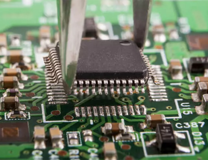
3.3 Core GNSS Chip Soldering
The GNSS main chip is the most precise and fragile component of the board, requiring strict temperature control during soldering. For BGA and QFN packaged GNSS chips (such as ZEDF9P), adopt reflow soldering with a standardized temperature curve to avoid chip damage:
Preheating stage: 160–180°C for 60–120 seconds to activate flux and evaporate moisture
Temperature rise stage: Heating rate controlled at 3°C/second to avoid thermal shock
Peak temperature: 245°C, maintained for 10–30 seconds to ensure full solder melting
Cooling stage: Uniform cooling at 3°C/second to enhance solder joint strength and stability
For manual soldering of small packaged chips, avoid prolonged hightemperature heating on the chip surface (heating time per pin ≤3 seconds) to prevent internal crystal oscillator and circuit damage. After soldering, use a magnifying lamp to inspect all pins for short circuits, open circuits, and cold solder joints.
3.4 RF Circuit and Antenna Interface Assembly
The RF circuit assembly stage determines the GNSS board’s signal reception capability, making it the most critical link in the entire assembly process. According to ublox official hardware integration specifications, the RF trace connecting the antenna interface to the GNSS chip must be as short as possible (preferably ≤30mm) to reduce signal attenuation and noise interference.
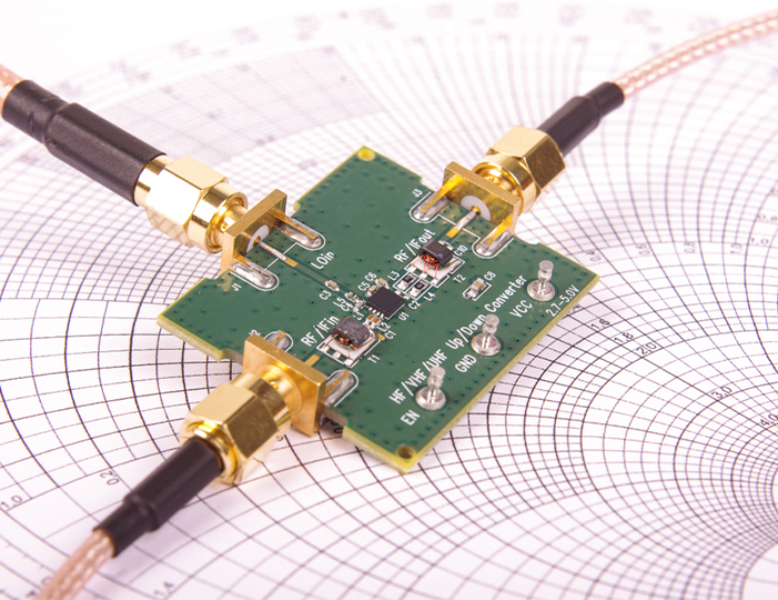
When assembling external antenna interfaces (SMA, IPEX, U.FL), ensure firm welding and complete 50Ω impedance matching. The LNA and SAW filter in the RF circuit must be accurately positioned and soldered to effectively filter out outofband interference signals and improve satellite signal sensitivity. It is strictly prohibited to place digital circuit components near RF traces to avoid electromagnetic crosstalk between digital signals and RF signals.
3.5 Power and Communication Circuit Assembly
Assemble LDO voltage regulators, power protection chips, and filter circuits to ensure stable 3.3V power output for the GNSS chip. Unstable power supply is the main cause of GNSS positioning drift and satellite loss of lock, so multiple filter capacitors must be configured at the power input and output terminals. Then solder UART, USB, and I2C communication interfaces, ensuring neat and full solder joints to guarantee stable data transmission.
Install the backup battery component to maintain the chip’s ephemeris data storage, which shortens the satellite hot start time and improves positioning response speed in subsequent use.
3.6 PostAssembly Cleaning and Drying
After completing all soldering work, thoroughly clean the board with ultrasonic cleaning equipment and isopropyl alcohol to remove residual flux, solder paste, and dust. Residual flux will corrode solder joints over time, causing circuit failure and signal instability. After cleaning, place the board in a constanttemperature drying oven for 30 minutes to completely evaporate cleaning solution moisture and prevent short circuits caused by residual water vapor.
4. Critical Design & Assembly Best Practices for GNSS Receiver Boards
To maximize GNSS board performance, professional assembly must follow industry best practices for RF layout, EMI shielding, thermal management, and component placement. These standardized rules distinguish highprecision industrial GNSS boards from ordinary consumergrade modules and directly improve positioning accuracy and stability.
4.1 RF Layout and Impedance Matching Standards
All RF transmission traces must strictly follow 50Ω impedance matching design and assembly standards. Do not arbitrarily change trace width or bend radian during assembly, as irregular traces will cause impedance mismatch, signal reflection, and serious signal attenuation. The RF ground plane must be complete and continuous without gaps to provide stable grounding for RF signals and reduce noise interference.
Isolate RF analog circuits from digital circuits completely during assembly. Use ground isolation grooves to separate highfrequency RF circuits from lowfrequency digital circuits and power circuits to avoid digital signal noise flooding weak satellite signals, which is a key factor affecting GNSS reception sensitivity.
4.2 EMI and AntiInterference Assembly Rules
GNSS satellite signals are extremely weak (nWlevel), so antiinterference design and assembly are essential. During assembly, highpower components such as power regulators and crystal oscillators must be placed far away from RF circuits and antenna areas. For highprecision RTK boards, install metal shielding covers on the RF circuit area after assembly to isolate external electromagnetic interference from power supplies, motors, and wireless communication equipment.
4.3 Thermal Management Optimization
Longterm hightemperature operation will cause GNSS chip frequency drift and positioning accuracy decline. During assembly, reserve heat dissipation space for core chips and power components. For industrialgrade boards, paste thermal conductive adhesive on the chip back to accelerate heat dissipation and ensure stable operation in hightemperature environments. Avoid component stacking and dense placement to prevent local overheating of the board.
4.4 Antenna Installation and Matching Guidelines
Antenna assembly and installation directly determine satellite signal reception quality. Always install the antenna before powering on the GNSS board to avoid RF circuit burnout caused by noload power supply. Use highquality lowloss coaxial cables to connect the antenna and receiver board, and minimize cable length to reduce signal loss.
For outdoor industrial applications, install the antenna on a metal ground plane (metal plate area ≥20cm) to enhance signal reception stability and suppress multipath interference. Ensure the antenna has an unobstructed sky view and avoid installation under metal shelters, buildings, or dense vegetation.
5. PostAssembly Inspection, Testing and Calibration
Assembly is not complete without strict quality inspection and performance testing. Postassembly verification ensures the GNSS board meets design specifications and industry standards, eliminating defective products before delivery and application. The testing process includes appearance inspection, electrical performance testing, and actual positioning performance calibration.
5.1 Visual and AOI Inspection
First conduct manual visual inspection with a magnifying lamp to check for solder joint defects, component misplacement, and residual debris. For mass production, use Automated Optical Inspection (AOI) equipment to intelligently detect solder bridges, missing components, offset placement, and cold solder joints, achieving highprecision and highefficiency quality screening.
5.2 Electrical Performance Testing
Use a multimeter to test board continuity, power supply voltage stability, and circuit onoff status to eliminate short circuits and open circuits. Use an RF impedance analyzer to verify 50Ω impedance matching of RF circuits to ensure no signal reflection loss. Test communication interface data transmission function to confirm normal output of positioning data.
5.3 GNSS Signal and Positioning Calibration
Place the assembled board in an open outdoor environment with unobstructed sky visibility for realscene positioning testing. Record key performance indicators including satellite number acquired, SNR value, hot/warm/cold start time, and positioning accuracy. Standard qualified parameters: stable reception of 18+ satellites, SNR ≥35dB, cold start time ≤60 seconds, and positioning error within design specifications.
For RTK highprecision boards, perform differential positioning calibration to verify centimeterlevel positioning accuracy and ensure stable fixed solution output in complex environments. Update and debug the latest firmware after assembly to optimize satellite acquisition algorithms and improve environmental adaptability.
6. Common GNSS Receiver Board Assembly Defects & Troubleshooting
Most GNSS performance failures stem from nonstandard assembly processes. Summarizing common defects and targeted solutions can effectively improve assembly yield and product stability. Below are the most frequent assembly faults and professional troubleshooting methods.
6.1 Slow Satellite Acquisition and Few Locked Satellites
Causes: Excessively long RF traces, impedance mismatch, poor antenna contact, residual flux interference, or nearby electromagnetic interference from assembled components.
Solutions: Recheck RF circuit soldering and trace integrity, clean residual flux thoroughly, refix antenna connections, adjust component placement to eliminate interference sources, and recalibrate RF impedance matching parameters.
6.2 Positioning Drift and Low Accuracy
Causes: Unstable power supply solder joints, virtual soldering of filter capacitors, poor grounding, or multipath interference caused by unreasonable antenna assembly.
Solutions: Resolder power and filter circuit components, reinforce board grounding, optimize antenna installation position and angle, and recalibrate positioning parameters to eliminate drift errors.
6.3 Intermittent Signal Loss and Data Disconnection
Causes: Loose solder joints of communication interfaces and RF interfaces, component virtual soldering, or static damage to core chips during assembly.
Solutions: Resolder all key interfaces and component pins, test chip operating status, replace staticdamaged components, and strengthen static protection in subsequent assembly processes.
6.4 Board Overheating and Short Circuit Failure
Causes: Excessive solder causing adjacent pad short circuits, component misplacement, or residual metal debris on the board surface after assembly.
Solutions: Clean the board thoroughly, eliminate short circuit points, replace damaged components, and standardize soldering operation specifications to avoid excessive solder volume and component placement errors.
7. Industrial Application Scenarios of HighQuality GNSS Receiver Board Assembly
Standardized GNSS receiver board assembly provides reliable hardware support for multiple highprecision positioning industries, and assembly process accuracy directly determines equipment operational stability:
Surveying and Mapping RTK Equipment: Highprecision assembly ensures centimeterlevel positioning accuracy for land surveying, engineering construction, and geographic information collection.
Drone Navigation: Antiinterference assembly technology guarantees stable positioning of UAVs in complex urban and mountainous environments, preventing flight deviation and crash risks.
Automotive Intelligent Driving: Reliable board assembly supports vehicle highprecision navigation, ADAS assisted driving, and automatic parking systems.
IoT Positioning Devices: Lowpower and highstability assembly design adapts to longterm operation of smart logistics, asset tracking, and smart city monitoring equipment.
Agricultural Precision Machinery: Antivibration and hightemperature resistant assembly processes meet the harsh working environment requirements of agricultural drones and intelligent farming equipment.
GNSS receiver board assembly is a systematic precision engineering process that integrates circuit soldering, RF optimization, antiinterference design, and performance calibration. Every step from preassembly static protection, standardized component placement, and strict temperaturecontrolled soldering to postassembly testing directly affects the final positioning performance and service life of GNSS equipment. Adhering to professional assembly specifications, optimizing RF circuit and antiinterference design, and completing comprehensive postassembly testing are the core keys to manufacturing highprecision, highstability GNSS receiver boards.
With the rapid development of intelligent navigation, autonomous driving, and smart IoT industries, the market demand for highperformance GNSS receiver boards continues to grow. Mastering standardized assembly processes and best practices helps electronics manufacturers and technical developers improve product yield, enhance market competitiveness, and provide reliable positioning hardware support for various highprecision navigation application scenarios.
Lucy Yang | lucy.y@toxutech.com
Dotty Zhao | sales04@toxutech.com
Global Business Director / Sales Team / Global Operations


 En
En Cn
Cn Korean
 Home >