

-
Products -PCBA Manufacturing RF Connectors RF Cable Assemblys Embedded Antennas External Antennas GNSS Positioning Solutions
RF Connectors

RF Cable Assemblys
Embedded Antennas
External Antennas
GNSS Positioning Solutions


 Language


Language


Time:2026-10-15 Views:0
GNSS antenna cable PCBA integration is the core engineering process that merges Global Navigation Satellite System (GNSS) antenna units, RF coaxial cables, and printed circuit board assembly (PCBA) circuitry into a high-performance, reliable positioning system. As GNSS technology becomes ubiquitous in consumer electronics, automotive navigation, industrial IoT, drone RTK, precision agriculture, and smart infrastructure, standardized and optimized antenna cable PCBA integration directly determines positioning accuracy, signal stability, noise resistance, and product service life. Poor integration design often leads to common issues such as low satellite signal lock rate, frequent positioning drift, high signal loss, electromagnetic interference (EMI), and even system failure in complex environments.
This comprehensive guide covers the fundamental principles, key design specifications, step-by-step integration workflows, component selection criteria, common pitfalls, testing validation methods, and advanced optimization strategies for GNSS antenna cable PCBA integration. Tailored for RF engineers, PCBA designers, product developers, and manufacturing technicians, this article adheres to Google SEO best practices by targeting high-intent keywords, solving core industry pain points, and providing actionable technical guidance for both passive and active GNSS antenna integration scenarios.
1. Core Overview of GNSS Antenna Cable PCBA Integration
1.1 Definition and Core Functions
GNSS antenna cable PCBA integration refers to the systematic engineering process of layout design, component soldering, cable docking, impedance matching, and anti-interference optimization for GNSS antenna interfaces, RF transmission cables, and PCBA main circuits. Unlike ordinary PCB wiring integration, GNSS RF systems have extremely strict requirements for signal integrity due to the weak nature of satellite navigation signals—GNSS satellite signals reach the ground with power levels as low as -130dBm, requiring zero-loss transmission and high noise suppression throughout the link.
The core functions of professional GNSS antenna cable PCBA integration include: stable transmission of GPS, Beidou, GLONASS, Galileo multi-band satellite signals, precise impedance matching of RF links, suppression of EMI and radio frequency interference (RFI), guarantee of low insertion loss and low voltage standing wave ratio (VSWR), and reliable mechanical connection between antenna cables and PCBA boards. It serves as the critical bridge between external GNSS antenna acquisition and internal chip signal demodulation and positioning calculation.
1.2 Key Application Scenarios
High-quality GNSS antenna cable PCBA integration is essential for all satellite positioning terminal devices, covering mainstream high-demand industries:
Automotive Electronics: Vehicle navigation, ADAS positioning, vehicle tracking, and intelligent driving terminals, which require high stability in high-temperature and strong electromagnetic interference vehicle environments.
Industrial IoT & Smart Devices: Smart meters, asset tracking terminals, wearable positioning devices, and industrial monitoring equipment with long-term outdoor operation requirements.
Precision Positioning Equipment: UAV RTK modules, agricultural navigation machinery, surveying and mapping instruments, and high-precision timing systems that demand centimeter-level positioning accuracy.
Consumer Electronics: Smart watches, tablet computers, portable navigators, and outdoor sports devices with miniaturized PCBA integration requirements.
Aerospace & Defense: Low-orbit satellite terminals, aviation navigation equipment, and military positioning systems with ultra-high reliability and anti-interference standards.
1.3 Key Technical Challenges in Integration
Most GNSS positioning failures stem from non-standard antenna cable PCBA integration rather than chip or antenna hardware defects. The main technical challenges include: strict 50Ω characteristic impedance control for RF links, signal attenuation caused by cable length and bending, EMI interference from PCB digital and power circuits, poor contact of antenna connectors, inconsistent grounding design, and signal-to-noise ratio (SNR) degradation in long-distance transmission. Solving these challenges is the core goal of standardized integration design and manufacturing.
2. Key Component Selection for GNSS Antenna Cable PCBA Integration
Component selection is the foundation of high-quality GNSS antenna cable PCBA integration. Matching antennas, RF cables, connectors, and PCBA auxiliary components according to application scenarios directly determines the upper limit of system performance. This section details the selection standards for core components applicable to Google high-traffic industry scenarios.
2.1 GNSS Antenna Selection: Passive vs Active Antennas
GNSS antennas are divided into passive antennas and active antennas, with completely different PCBA integration schemes, which must be distinguished in design:
Passive GNSS Antennas: Purely structural antenna units without built-in amplification devices, featuring low cost, small size, and simple integration. They are suitable for short cable transmission (within 10cm) and low-interference indoor scenarios. Passive antennas rely entirely on PCBA front-end circuits to compensate for signal loss, requiring strict control of PCB trace loss and impedance matching. They are widely used in low-power consumer miniature devices.
Active GNSS Antennas: Integrated with low-noise amplifier (LNA) and SAW filter modules, which can amplify weak satellite signals and filter out-band interference. Professional active antennas support long-distance cable transmission and complex electromagnetic environments. According to industry standards, when the antenna-to-receiver cable length exceeds 10cm or requires long coaxial runs, an LNA + SAW filter configuration is mandatory to offset coax loss and preserve SNR. Active antennas usually adopt 5V DC power supply through coaxial cable via a bias-T circuit on the PCBA, which is the key point of active antenna PCBA integration.
For high-precision RTK and outdoor industrial equipment, multi-band active GNSS antennas supporting L1/L2/L5 full-band reception are preferred to ensure multi-system satellite fusion positioning stability.
2.2 GNSS RF Cable Selection Standards
RF coaxial cables are the signal transmission medium between the antenna and PCBA, and their specifications directly determine insertion loss and signal stability. The core selection parameters include impedance, cable type, length, bending resistance, and environmental adaptability.
All GNSS systems follow the unified 50Ω characteristic impedance standard, so all selected cables must maintain strict 50Ω impedance consistency to avoid impedance mismatch caused signal reflection and VSWR surge. Common mainstream cable models include LMR-100, RG-174, RG-58, and ultra-thin FAKRA cables for automotive use.
In terms of loss control: for cable lengths within 5 meters, 15dB receiver gain is sufficient to maintain normal signal reception without an onboard LNA; for lengths exceeding 5 meters, high-gain active antennas or secondary amplification circuits must be configured to compensate for line loss. In PCBA integration, the antenna cable layout should minimize bending and stretching, and avoid sharp bends that damage the internal shielding layer, which will cause signal leakage and interference.
2.3 Antenna Connector Selection for PCBA Docking
Connectors are the key docking components between cables and PCBA boards, and poor connector matching and installation are common causes of positioning instability. The mainstream GNSS antenna PCBA connectors in the market include SMA, MMCX, MCX, U.FL, and FAKRA, with differentiated application scenarios:
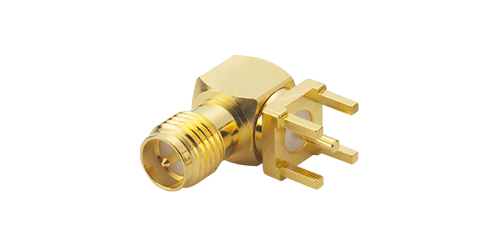
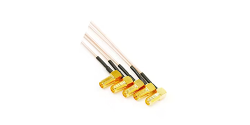
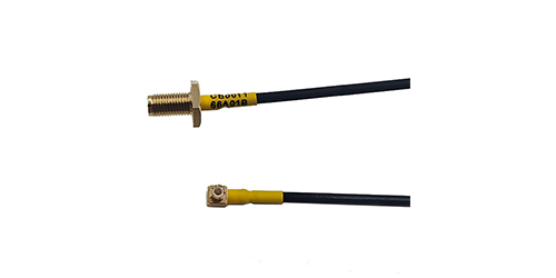
SMA Connectors: Threaded, high mechanical stability, wide mating cycle range, excellent waterproof and dustproof performance. Ideal for outdoor industrial equipment, automotive navigation, and fixed-position devices. IP67 waterproof SMA bulkhead connectors are recommended for outdoor scenarios to resist rain and dust erosion.
MMCX/MCX Connectors: Miniature push-on connectors with small size and easy assembly, suitable for miniaturized PCBA products such as wearable devices and portable terminals. Note that frequent plugging and unplugging may cause loose contact, so strain relief structures are required in integration.
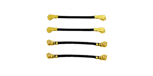
U.FL Connectors: Ultra-small high-frequency connectors, the first choice for high-density miniature PCBA integration, widely used in drone modules and IoT miniature positioning terminals.
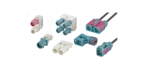
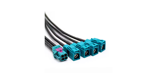
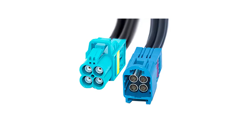
FAKRA Connectors: Special automotive-grade connectors with anti-vibration and high-temperature resistance, exclusively used for vehicle GNSS antenna PCBA integration to adapt to vehicle vibration and high-temperature working environments.
Connector installation must follow standardized processes: use calibrated torque wrenches for locking to avoid excessive or insufficient force, add strain relief structures to prevent bending moment damage to connectors, and equip panel gaskets to meet IP protection level requirements.
3. Professional PCBA Layout Design for GNSS Antenna Cable Integration
PCB layout design is the core link of GNSS antenna cable PCBA integration, which determines the inherent performance of the RF link. All layout designs must focus on impedance matching, signal integrity, anti-interference, and loss minimization, with strict compliance with the following industry-standard specifications.
3.1 50Ω Impedance Matching Design
Impedance matching is the top priority of GNSS RF PCBA design. Any deviation from the 50Ω standard will cause signal reflection, increase VSWR, reduce signal reception efficiency, and even lead to satellite lock failure. The antenna feed trace from the PCBA connector pad to the GNSS chip RF pin must maintain continuous 50Ω impedance throughout the whole process.
For conventional FR4 PCB substrates, designers can calculate trace width, copper thickness, and dielectric layer spacing according to substrate dielectric constant parameters to achieve accurate impedance control. For coplanar waveguide (CPW) layout scenarios (suitable for thin PCB boards and limited layout space), the ground gap on both sides of the trace needs precise adjustment to ensure impedance stability. It is strictly forbidden to randomly widen or narrow the RF trace, and no via holes or branch traces are allowed on the main antenna signal path.
3.2 Ground Plane Design Specifications
A complete and continuous ground plane is the basis for GNSS signal anti-interference and impedance stability, and is not optional for patch antenna integration. A complete ground plane must be reserved directly below the entire antenna RF trace and connector area, with a ground margin of no less than 0.5mm on both sides of the trace to avoid ground discontinuity causing signal leakage.
It is forbidden to arrange digital traces, power traces, and via holes in the ground plane under the antenna RF area. The ground plane of the antenna area is independently grounded and connected to the main board ground through a single-point grounding method to prevent high-frequency noise from digital circuits and switching power supplies from coupling into the GNSS signal link. For high-precision positioning products, partial shielding (Faraday shield) can be added to the antenna circuit area to further isolate external EMI interference.
3.3 Trace Layout and Anti-Interference Design
The GNSS antenna RF trace must follow the principles of "shortest, straightest, and cleanest". The optimal trace length is controlled within 20mm; excessively long traces will inevitably increase insertion loss and introduce interference. The RF path should be independent and isolated, with a spacing of more than 3mm from high-speed digital traces, switching regulator circuits, and power modules to avoid cross-interference.
In active antenna integration, the bias-T power supply circuit for antenna power supply needs to be arranged away from the RF main path, and high-frequency filter capacitors are matched to suppress power supply ripple noise. The SAW filter and LNA devices on the PCBA should be placed close to the antenna connector to filter interference and amplify signals at the front end of the link, maximizing the guarantee of SNR.
3.4 Multi-Band GNSS Compatibility Design
Modern GNSS terminals support multi-system fusion positioning (GPS, Beidou, GLONASS, Galileo), so PCBA integration needs to meet multi-band signal transmission requirements. The RF link design must cover L1, L2, L5 and other mainstream frequency bands, with flat insertion loss in the full frequency band to avoid signal attenuation deviation of different satellite systems. The antenna cable and connector must also support multi-band high-frequency transmission to ensure no performance degradation in wide-frequency operation.
4. Standard GNSS Antenna Cable PCBA Assembly Process
Scientific and standardized assembly processes ensure the consistency and reliability of mass-produced products. Non-standard assembly operations are the main cause of unstable product performance and low yield. The complete integration assembly process is divided into PCB pre-processing, component soldering, cable docking, grounding processing, and post-assembly inspection.
4.1 PCB Pre-Processing and Inspection
Before assembly, inspect the PCB board for flaws such as trace breakage, solder mask peeling, and ground plane discontinuity. Verify that the impedance of the reserved antenna RF path meets the 50Ω standard via professional testing equipment. Clean the pad area of the antenna connector to remove dust, oil, and oxide layers to ensure firm soldering and good conductivity. For boards that have been stored for a long time, baking and dehumidification treatment is required to avoid soldering voids caused by moisture.
4.2 Core Component Soldering Process
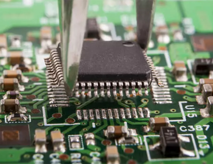
Soldering of antenna connectors, LNA, SAW filters, and bias-T circuits needs to adopt precision soldering processes. The connector pins must be fully aligned with PCB pads, with uniform solder volume to avoid virtual soldering, cold soldering, and solder bridging. Excessive solder will cause impedance mutation, while insufficient solder will lead to poor contact and increased contact resistance.
For miniature connectors such as U.FL and MMCX, constant-temperature precision soldering stations are used to control the temperature at 320-350℃ to avoid high-temperature damage to connector insulation layers and PCB substrates. After soldering, use a magnifying glass to inspect the welding points one by one to ensure no hidden soldering defects.
4.3 Antenna Cable Docking and Fixing
When docking the coaxial cable with the PCBA connector, ensure accurate alignment and in-place locking. For threaded SMA connectors, use a calibrated torque wrench for locking to standard torque to avoid loose connection or thread damage. For push-on miniature connectors, confirm the clamping sound to ensure complete in-place docking.
After docking, fix the cable with glue or fixing clips to avoid cable shaking and connector loosening caused by equipment vibration. Set aside a reasonable cable margin according to the product structure to prevent cable tension and bending damage during assembly and use. For outdoor and vehicle products, perform overmold protection on the cable connector root to improve tensile and waterproof performance.
4.4 Grounding and Shielding Integration
Complete grounding treatment is required after cable docking. The antenna cable shielding layer must be reliably connected to the PCBA ground plane to form a complete shielding system, which can effectively isolate external electromagnetic interference and prevent internal signal leakage. It is forbidden to suspend the cable shielding layer, which will cause serious signal noise increase and positioning drift.
For high-interference working environments, install metal shielding covers on the PCBA antenna circuit area to form a closed shielding space, completely isolating the interference of power circuits and digital circuits on GNSS weak signals.
5. Key Testing and Validation Methods After Integration
Post-integration testing is a necessary link to verify the quality of GNSS antenna cable PCBA integration, which can effectively eliminate defective products and ensure batch consistency. The core testing items include RF parameter testing, signal performance testing, and environmental reliability testing.
5.1 RF Basic Parameter Testing
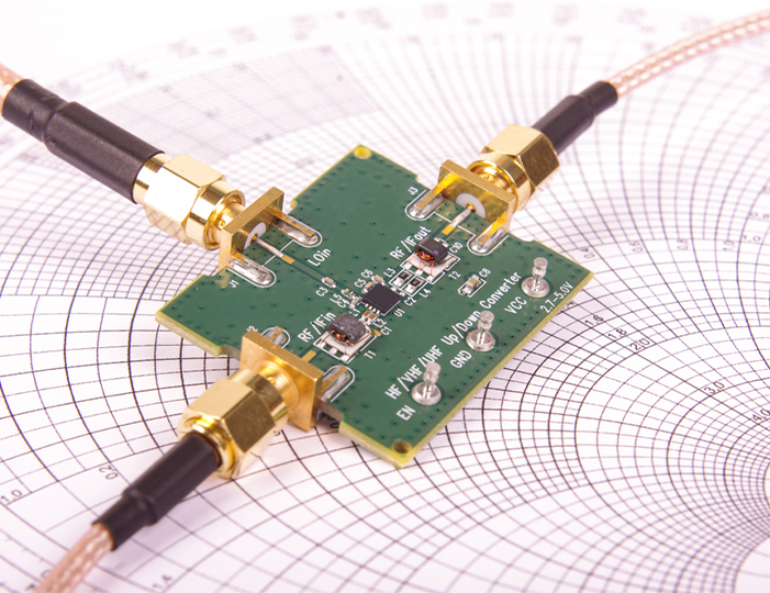
Use a vector network analyzer (VNA) to test core RF parameters of the integrated link, including S11 return loss, S21 insertion loss, and VSWR. Qualified GNSS integration links require VSWR < 1.5, return loss > 14dB, and low insertion loss in the full frequency band. Excessive VSWR indicates impedance mismatch, which requires rechecking PCB layout and connector soldering quality.
At the same time, conduct continuity testing and pull testing of cable assemblies to verify the firmness of welding and docking, and eliminate hidden dangers of poor contact and loose cables.
5.2 Satellite Signal Performance Testing
Signal performance is the most intuitive evaluation index of integration quality. Professional GNSS signal testers are used to test key indicators such as carrier-to-noise ratio (CN0), satellite lock number, positioning success rate, and positioning accuracy. Industry optimal standard: the average CN0 value reaches more than 40 dB-Hz in a benign environment; a 3dB decrease in CN0 means obvious attenuation of the RF link, which requires troubleshooting and optimization.
Simulate multiple working scenarios including static placement, dynamic movement, and sheltered environments to test signal stability, and verify whether there are problems such as signal dropout and positioning drift.
5.3 Environmental Reliability Testing
For industrial and vehicle-grade products, environmental reliability testing must be carried out after integration, including high and low temperature cycling test, vibration test, waterproof and dustproof test, and long-term aging test. Verify whether the antenna cable connection and PCBA circuit performance remain stable under extreme working conditions to ensure long-term reliable operation of the product.
6. Common Integration Mistakes and Optimization Solutions
In actual engineering development and mass production, most GNSS performance problems are caused by standardized integration errors. This section summarizes the most common mistakes and targeted optimization solutions to help engineers quickly troubleshoot and improve integration quality.
6.1 Impedance Mismatch Causing Signal Reflection
Mistake: Random modification of RF trace width, incomplete ground plane, unreasonable via hole setting, and mismatched cable impedance lead to 50Ω link deviation, resulting in signal reflection and increased loss.
Optimization Solution: Strictly design trace parameters according to PCB substrate parameters, keep the RF trace complete and straight, prohibit random via holes and branches, ensure continuous ground plane, and select full 50Ω standard cables and connectors to realize full-link impedance matching.
6.2 Insufficient Anti-Interference Design Leading to Low SNR
Mistake: The antenna RF area is close to high-power and high-speed circuits, no independent shielding and grounding design, and power supply ripple interference leads to reduced satellite signal SNR and frequent positioning drift.
Optimization Solution: Partition PCB layout, isolate RF area from digital and power areas, adopt single-point grounding for antenna circuits, add LNA and SAW filter front-end filtering and amplification, and install shielding covers for high-interference scenarios.
6.3 Unreasonable Cable Layout and Docking
Mistake: Excessively long cables, sharp bending, loose connector docking, ungrounded shielding layer, and no strain relief structure lead to signal leakage and unstable contact.
Optimization Solution: Shorten the cable length as much as possible, avoid sharp bending, standardize connector locking and fixing, reliably ground the shielding layer, and add strain relief and waterproof protection structures.
6.4 Mismatched Active and Passive Antenna Integration Schemes
Mistake: Using passive antennas for long-distance cable transmission resulting in excessive signal loss, or missing bias-T power supply circuits for active antennas leading to abnormal antenna operation.
Optimization Solution: Match antenna types according to cable length and application environment; configure bias-T power supply and filter circuits for active antenna PCBA integration, and add LNA amplification compensation for long-distance transmission scenarios.
7. Advanced Optimization Trends for GNSS Antenna Cable PCBA Integration
With the rapid development of high-precision positioning, miniaturization, and low-power GNSS devices, GNSS antenna cable PCBA integration technology is also constantly iterating. The current industry development trends focus on miniaturized high-density integration, ultra-low loss RF link design, intelligent anti-interference, and high-reliability industrial-grade integration.
First, miniaturized integration: With the popularization of wearable devices and miniature IoT terminals, ultra-thin PCB design, embedded antenna integration, and integrated cable-connector assembly have become mainstream, realizing smaller size and lighter weight while ensuring RF performance.
Second, high-precision loss optimization: For RTK centimeter-level positioning equipment, the industry adopts ultra-low loss cable materials, high-precision impedance PCB design, and full-link shielding technology to minimize signal loss and noise interference, meeting ultra-high positioning accuracy requirements.
Third, intelligent anti-interference integration: The new generation of PCBA integration schemes integrates adaptive filtering modules and multi-frequency anti-jamming circuits, which can automatically suppress complex environmental interference and improve the stability of GNSS signals in urban sheltered, high-rise, and strong electromagnetic interference scenarios.
Fourth, standardized modular integration: Industry manufacturers are gradually promoting standardized GNSS antenna cable PCBA modular solutions, realizing plug-and-play assembly, improving mass production efficiency, and reducing product consistency errors.
GNSS antenna cable PCBA integration is a systematic precision engineering technology covering component selection, PCB layout, assembly process, performance testing, and reliability optimization. Its technical level directly determines the positioning accuracy, signal stability, and service life of GNSS terminal equipment. In the context of the rapid development of intelligent navigation, industrial IoT, and autonomous driving, standardized and high-precision GNSS antenna cable PCBA integration has become a key technical indicator for measuring product competitiveness.
Enterprises and engineers should strictly follow RF design specifications, select matching components according to application scenarios, standardize assembly processes, and conduct comprehensive performance testing and reliability verification. By avoiding common integration mistakes and adopting advanced optimization schemes, they can effectively improve GNSS signal reception quality, eliminate positioning failures and drift problems, and create high-reliability satellite positioning terminal products suitable for complex industrial and consumer scenarios.
FAQs About GNSS Antenna Cable PCBA Integration
Q1: What is the most critical parameter for GNSS antenna PCBA integration?
The 50Ω full-link impedance matching is the most critical parameter. Any impedance mismatch will cause signal reflection, increased VSWR, and reduced signal reception efficiency, which is the primary cause of poor GNSS positioning performance.
Q2: Do I need an LNA for short GNSS antenna cable integration?
For cable lengths within 10cm in low-interference environments, passive antennas without LNA can meet the demand. For cables longer than 10cm or high-interference scenarios, LNA + SAW filter configuration is required to compensate for line loss and suppress noise.
Q3: Why does GNSS positioning drift after PCBA integration?
The main reasons include incomplete PCB ground plane, RF trace interference from power/digital circuits, loose antenna cable connectors, ungrounded cable shielding layer, and insufficient front-end signal filtering and amplification. Targeted optimization of integration design and process can solve the problem.
Q4: Which connector is best for automotive GNSS PCBA integration?
FAKRA automotive-grade connectors are the optimal choice, with excellent vibration resistance, high-temperature resistance, and waterproof performance, fully adapting to the complex working environment of vehicle terminals.
Lucy Yang | lucy.y@toxutech.com
Dotty Zhao | sales04@toxutech.com
Global Business Director / Sales Team / Global Operations


 En
En Cn
Cn Korean
 Home >