

-
Products -PCBA Manufacturing RF Connectors RF Cable Assemblys Embedded Antennas External Antennas GNSS Positioning Solutions
RF Connectors

RF Cable Assemblys
Embedded Antennas
External Antennas
GNSS Positioning Solutions




 Language


Language


Time:2026-10-15 Views:0
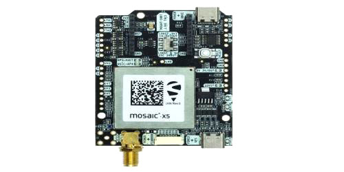
Custom GNSS PCB board assembly is a specialized printed circuit board assembly process tailored for Global Navigation Satellite System (GNSS) devices, including GPS, GLONASS, Galileo, BeiDou, and QZSS positioning systems. Unlike standard PCB assembly, custom GNSS PCBA requires strict RF signal control, highprecision component placement, optimized grounding design, and rigorous quality testing to ensure stable satellite signal reception, accurate positioning, and longterm operational reliability. As GNSS technology penetrates autonomous vehicles, IoT tracking devices, aerospace equipment, marine navigation systems, and smart agricultural machinery, professional custom GNSS PCB board assembly has become a core foundation for highperformance positioning product development. This comprehensive guide explores the core processes, key technical requirements, industry best practices, quality control standards, application scenarios, and selection tips for custom GNSS PCB assembly, helping businesses and engineers acquire reliable custom navigation PCBA solutions.
1. What Is Custom GNSS PCB Board Assembly?
Custom GNSS PCB board assembly refers to the customized manufacturing and assembly service of PCB circuits dedicated to GNSS positioning hardware. It covers the entire workflow from customized PCB design optimization, component procurement, SMT/DIP assembly, soldering, inspection, functional testing to final packaging and delivery. Different from universal PCB assembly, GNSSbased PCBA focuses heavily on RF signal integrity, low noise interference, controlled impedance, and highprecision positioning performance, which are the key differentiators of professional GNSS circuit assembly.
Standard PCB assembly only meets basic circuit conduction requirements, while custom GNSS PCB board assembly is optimized for the unique working characteristics of satellite navigation modules. GNSS devices need to capture weak satellite signals in complex electromagnetic environments, so every link from PCB substrate selection, trace layout, antenna circuit assembly to shielding processing must be strictly customized. Customization supports diverse product demands, including lowpower portable GNSS trackers, highprecision RTK positioning boards, industrialgrade antivibration navigation PCBs, and aerospacelevel ultrahighstability GNSS circuit boards.
Core customized dimensions of GNSS PCB assembly include customized circuit stackup design, 50Ω RF impedance control, customized antenna placement schemes, customized antiinterference shielding assembly, lowpower circuit optimization, and customized functional testing procedures according to client product scenarios. This highly tailored service ensures that the final PCBA products can adapt to different environmental conditions and positioning accuracy requirements, covering consumer, industrial, automotive, marine, and aerospacegrade applications.
2. Core Technical Requirements for Custom GNSS PCB Assembly
GNSS positioning accuracy and signal stability directly depend on the assembly quality and technical optimization of the PCB board. Professional custom GNSS PCB board assembly must comply with strict RF and electronic design specifications, with the following core technical requirements that cannot be ignored.
2.1 Strict 50Ω Controlled Impedance Design and Assembly
RF signal transmission of GNSS modules relies on standardized 50Ω characteristic impedance circuits, which is the most critical technical index of GNSS PCB assembly. Uncontrolled impedance will cause signal reflection, attenuation, and distortion, resulting in weak satellite signal reception, slow positioning, and large positioning errors. In custom GNSS PCB assembly, manufacturers must strictly follow impedance design specifications, including customized trace width, spacing, PCB stackup structure, and dielectric material parameters.
During the assembly process, it is necessary to ensure that all RF channel components, including antennas, filters, amplifiers, and GNSS module pins, are perfectly matched with the 50Ω impedance circuit. Any deviation in soldering or component placement will damage impedance consistency. Professional assembly teams will reserve impedance test coupons on the PCB and conduct impedance testing after assembly to ensure full compliance with design standards, effectively reducing RF signal loss.
2.2 Optimized Antenna Circuit Placement and Assembly
Antenna performance determines the signal capture capability of GNSS devices, so antenna area assembly is the top priority of custom GNSS PCB board assembly. The antenna circuit area must be completely isolated from highfrequency noise sources such as MCU chips, power management modules, and crystal oscillators. During component placement, avoid metal component shielding and dense circuit stacking in the antenna radiation area to prevent signal blocking and electromagnetic interference.
All antenna pad soldering must be full and flat without virtual soldering or solder bridging. The assembly process strictly controls the height and position of antenna accessories to ensure unobstructed signal radiation. For builtin ceramic antennas and external antenna interfaces, standardized assembly processes are adopted to guarantee stable connection and minimize signal attenuation. Meanwhile, the antenna grounding design is optimized during assembly to form a complete grounding loop and improve antiinterference ability.
2.3 LowNoise Grounding and AntiInterference Assembly
GNSS satellite signals are extremely weak, susceptible to interference from power noise, highfrequency circuits, and external electromagnetic signals. Therefore, lownoise grounding design and standardized antiinterference assembly are essential for custom GNSS PCB assembly. The PCB adopts a multilayer grounding structure, with a complete ground layer to isolate RF signals from digital and power circuits.
During assembly, separate grounding processing is implemented for RF circuits, digital circuits, and power circuits to avoid commonground noise interference. Highprecision soldering is used for grounding pads to ensure low grounding resistance and stable conduction. For highnoise components such as power ICs and switching circuits, independent shielding covers are assembled to isolate noise. In addition, professional shielding paste and shielding assembly processes are applied in key RF areas to further improve the antiinterference performance of the GNSS board.
2.4 HighPrecision Component Placement and Solder Process Control
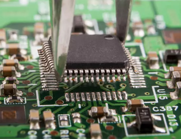
GNSS PCBA involves a large number of miniature precision components, including QFNpackaged GNSS modules, tiny resistors and capacitors, RF filters, and lownoise amplifiers. These components have high requirements for placement accuracy and soldering temperature. Custom GNSS PCB board assembly adopts highprecision SMT placement equipment with a placement accuracy of ±0.02mm to ensure accurate alignment of component pins and PCB pads.
The reflow soldering process strictly follows the temperature curve specifications for navigation circuit boards: preheating temperature controlled at 160–180°C for 60–120 seconds, heating rate maintained at 3°C/second, peak soldering temperature stabilized at 245°C for 10–30 seconds, and cooling rate controlled at 3°C/second. This standardized temperature curve effectively prevents component thermal damage, ensures full and reliable solder joint formation, and avoids solder bridging, missing solder, and virtual solder defects that affect GNSS performance.
3. Complete Process Flow of Custom GNSS PCB Board Assembly
Professional custom GNSS PCB board assembly follows a standardized, fulllink process flow from preproduction preparation to final delivery, ensuring zero defects in product quality and stable and consistent performance. The complete assembly process is divided into 8 core stages.
3.1 PreProduction Design Review and DFM Verification
Before formal assembly, the technical team conducts indepth review of customer’s GNSS PCB design files, including schematic diagrams, PCB layout files, stackup parameters, impedance requirements, and component BOM lists. DFM (Design for Manufacturability) optimization is carried out for navigation circuit characteristics, checking unreasonable layout risks such as too narrow RF traces, insufficient antenna isolation space, and unreasonable component spacing. Potential assembly difficulties and performance hidden dangers are eliminated in advance to ensure that the design scheme meets mass production and precision assembly requirements.
3.2 Precision Component Procurement and Inspection
GNSS positioning performance depends on the quality of core components. We adopt firstline brand GNSS modules, RF devices, and industrialgrade electronic components, and conduct 100% incoming inspection for all materials. The inspection items include component model verification, appearance inspection, electrical performance testing, and batch consistency detection. Fake and inferior components and parts with parameter deviations are strictly eliminated to avoid affecting positioning accuracy and product stability. For customized special components, professional sourcing channels are used to ensure material matching and supply stability.
3.3 Solder Paste Printing and Stencil Customization
A customized precision stencil is manufactured according to the GNSS PCB pad distribution characteristics, with optimized stencil opening size and thickness for miniature RF components and finepin modules to ensure uniform and appropriate solder paste printing. Solder paste with high conductivity and low residue is specially selected for GNSS RF circuits to reduce signal interference caused by solder paste residues. The printing process strictly controls pressure, speed, and alignment accuracy to prevent insufficient solder, excessive solder, and printing offset.
3.4 HighPrecision SMT Component Placement
Fullautomatic highspeed SMT placement equipment is used for component mounting, with separate parameter setting for GNSS core modules, RF components, and ordinary electronic components. Precision placement is realized for tiny chips and finepitch devices to ensure accurate pin alignment. Special protection is adopted for sensitive GNSS modules to avoid mechanical damage during placement. After placement, manual sampling inspection is matched to check component polarity, position, and placement accuracy to prepare for reflow soldering.
3.5 Standardized Reflow Soldering
According to the exclusive temperature curve of GNSS PCB assembly, fullautomatic reflow soldering is completed. The segmented temperature control mode ensures uniform heating of the circuit board, avoids local overheating damaging precision RF components, and ensures firm and full solder joints. After soldering, the board is cleaned with professional cleaning agent to remove flux residues, preventing residual impurities from causing circuit short circuits or signal attenuation.
3.6 MultiDimensional Quality Inspection
Multilevel inspection procedures are adopted for custom GNSS PCB board assembly to fully guarantee product quality, including AOI automated optical inspection, Xray inspection, ICT incircuit testing, and FCT functional testing. AOI equipment scans the entire board to detect solder bridges, missing solder, component offset, and polarity errors. Xray inspection detects hidden solder joint defects of BGA and QFN packaged GNSS modules that cannot be observed by naked eyes.
ICT incircuit testing checks circuit conduction, short circuit, open circuit, and component parameter abnormalities. FCT functional testing simulates actual working scenarios to verify GNSS satellite signal searching speed, positioning accuracy, signal stability, and power consumption performance. All unqualified products are screened out and reworked strictly in accordance with standardized procedures.
3.7 Aging Test and Environmental Adaptation Testing
For industrial and automotivegrade custom GNSS PCBA products, 24–72 hours of continuous aging testing is carried out to verify product stability under longterm working conditions. Meanwhile, environmental adaptation tests including high and low temperature resistance, vibration resistance, and humidity resistance are conducted according to application scenarios to ensure that the circuit board can maintain stable positioning performance in harsh environments such as high temperature, low temperature, vibration, and high humidity.
3.8 Finishing, Packaging and Delivery
After all tests are qualified, the circuit board undergoes final cleaning, appearance finishing, and antistatic packaging. Independent antistatic bags and shockproof packaging materials are used to avoid electrostatic damage and mechanical vibration damage during transportation. Batch product inspection reports, test data sheets, and assembly process documents are provided to customers to realize traceable product quality.
4. Key Challenges and Solutions in Custom GNSS PCB Assembly
Compared with ordinary PCB assembly, custom GNSS PCB board assembly faces unique technical challenges in RF signal control, antiinterference, and precision assembly. Summarizing industry pain points and targeted solutions helps improve product yield and performance.
4.1 Weak Satellite Signal and Low Positioning Accuracy
This problem is mainly caused by unreasonable RF trace layout, impedance mismatch, excessive solder residue, or antenna interference. The solution is to strictly implement 50Ω impedance control in the assembly process, optimize antenna area isolation, thoroughly clean postsoldering residues, and avoid highnoise component stacking near RF circuits. At the same time, calibrate RF signal channels during functional testing to ensure optimal signal transmission efficiency.
4.2 Electromagnetic Interference Affecting Stability
GNSS circuits are extremely sensitive to electromagnetic interference from power circuits, digital circuits, and external equipment. The core solution is to adopt separate grounding design, assemble professional shielding covers for noise sources, optimize power filter circuit assembly, and reduce power ripple interference. In addition, use highshielding PCB substrates and lowinterference assembly materials to improve the overall antiEMI performance of the board.
4.3 High Component Damage Rate and Low Yield
GNSS precision modules and RF components are heatsensitive and easily damaged by excessive soldering temperature or improper operation. The solution is to customize exclusive reflow temperature curves for GNSS products, equip professional precision assembly tools, and train professional technical teams familiar with navigation circuit characteristics. Strict incoming inspection and process monitoring are implemented to reduce component damage and improve assembly yield to over 99%.
5. Main Application Scenarios of Custom GNSS PCB Board Assembly
Custom GNSS PCB assembly products are widely used in precision positioning scenarios in various industries, covering consumer electronics, industrial control, automotive electronics, marine navigation, aerospace, and smart IoT fields. Different scenarios have customized requirements for PCBA accuracy, power consumption, stability, and environmental resistance.
5.1 Consumer IoT Tracking Devices
Portable GPS trackers, pet locators, vehicle antilost devices, and personal positioning terminals require lowpower, miniaturized custom GNSS PCBA solutions. The assembly process focuses on miniaturized layout optimization, lowpower circuit assembly, and lightweight design, ensuring stable positioning function while reducing product volume and power consumption, adapting to longterm batterypowered working modes.
5.2 Automotive and Autonomous Driving Systems
Automotive GNSS navigation boards and autonomous vehicle positioning modules require automotivegrade antivibration, hightemperature resistance, and high stability. Custom GNSS PCB board assembly strictly follows AECQ100 automotive electronic standards, adopts hightemperature resistant substrates and vibrationresistant assembly processes, and optimizes antiinterference performance to adapt to complex electromagnetic environments inside vehicles, ensuring realtime and accurate vehicle positioning.
5.3 Industrial Precision RTK Positioning Equipment
Industrial surveying and mapping, smart agriculture, and engineering construction equipment adopt RTK highprecision GNSS positioning technology, requiring centimeterlevel positioning accuracy. Custom PCBA assembly optimizes RF signal amplification and filtering circuits, improves signal antiinterference ability in complex industrial environments, and supports multisystem fusion positioning of GPS, BeiDou, and Galileo to meet highprecision industrial operation requirements.
5.4 Marine and Aerospace Navigation Equipment
Marine ships, drones, and aerospace equipment require ultrahigh stability and ultralow failure rate GNSS circuit boards. Custom assembly adopts aerospacegrade materials, enhanced shielding and anticorrosion processes, and extreme environmental resistance testing to adapt to highaltitude, highhumidity, strongelectromagnetic interference working environments, ensuring longterm reliable operation of navigation systems.
5.5 Smart City and Intelligent Transportation Systems
Traffic monitoring, vehicle scheduling, and smart street lamp positioning systems in smart cities rely on highstability GNSS positioning PCBA. Custom assembly realizes lowlatency positioning signal output, multidevice compatibility, and longterm outdoor environmental resistance, supporting 24hour uninterrupted stable operation of smart city positioning equipment.
6. How to Choose a Reliable Custom GNSS PCB Assembly Manufacturer?
The performance of GNSS products is directly determined by the technical strength and process level of the assembly manufacturer. When selecting a custom GNSS PCB board assembly supplier, enterprises need to focus on the following core indicators to avoid quality risks.
First, verify professional GNSS assembly technical experience. Ordinary PCB manufacturers lack RF signal control and navigation circuit assembly experience, which cannot meet highprecision positioning requirements. Professional manufacturers have mature GNSS PCBA process systems, exclusive soldering temperature curves, and RF testing standards.
Second, check complete quality testing capabilities. Reliable suppliers are equipped with AOI, Xray, ICT, FCT fullprocess testing equipment, and can provide customized functional testing and aging testing services according to customer scenarios, with complete test data reports.
Third, confirm customized service capabilities. Excellent manufacturers support personalized customization of PCB stackup, impedance parameters, circuit functions, and testing procedures, and can provide DFM design optimization suggestions to help customers optimize product performance and reduce costs.
Fourth, evaluate production efficiency and aftersales service. Formal manufacturers have standardized production lines, stable delivery cycles, and professional technical aftersales teams, which can quickly respond to customer modification demands and product quality problems, providing longterm technical support.
7. Future Development Trends of Custom GNSS PCB Board Assembly
With the rapid development of Beidou highprecision positioning, IoT, autonomous driving, and smart manufacturing technologies, custom GNSS PCB board assembly is evolving towards high precision, miniaturization, low power consumption, multisystem fusion, and high antiinterference.
First, highprecision RTK positioning PCBA will become mainstream. With the popularization of centimeterlevel positioning applications in smart agriculture, surveying and mapping, and autonomous driving, more customized assembly optimizations will be carried out for RTK differential positioning circuits to improve positioning accuracy and realtime performance.
Second, miniaturized and highly integrated assembly technology will be widely applied. Through advanced SMT microassembly technology and integrated module design, the volume of GNSS circuit boards will be further reduced, adapting to the miniaturization development trend of portable positioning devices.
Third, multiconstellation fusion positioning assembly optimization will be upgraded. Future GNSS PCBA will support simultaneous reception and fusion calculation of GPS, BeiDou, Galileo, and GLONASS multisatellite systems, requiring more precise RF circuit matching and multichannel signal antiinterference assembly technology.
Fourth, intelligent testing and automated production will improve industry standards. The popularization of AI intelligent detection and fullautomatic assembly lines will further improve the yield rate and consistency of custom GNSS PCB board assembly, reduce human error, and promote the standardized development of the industry.
Custom GNSS PCB board assembly is a highprecision, technically specialized electronic manufacturing service that integrates RF signal optimization, precision soldering, antiinterference design, and strict quality testing. It is not only the core hardware foundation of all satellite positioning equipment but also a key link to determine product positioning accuracy, signal stability, and service life. Different from ordinary PCB assembly, custom GNSS PCBA requires indepth professional accumulation in impedance control, antenna assembly, noise suppression, and scenariobased customization.
With the continuous expansion of GNSS application scenarios in smart transportation, industrial intelligence, IoT tracking, and aerospace fields, the market demand for highquality customized GNSS PCB assembly services will continue to grow. Choosing a professional, experienced, and fully tested custom GNSS PCB assembly manufacturer can effectively help enterprises reduce product research and development risks, improve product market competitiveness, and realize stable mass production of highprecision navigation positioning equipment.
Lucy Yang | lucy.y@toxutech.com
Dotty Zhao | sales04@toxutech.com
Global Business Director / Sales Team / Global Operations


 En
En Cn
Cn Korean
 Home >